


Application Technology
Understand cutting-edge application technology
Application Technology
Application of Gold in High-end Manufacturing-Electronic Semiconductor
- Categories:Application Technology
- Author:UMM
- Origin:
- Time of issue:2023-12-01 09:15
- Views:0
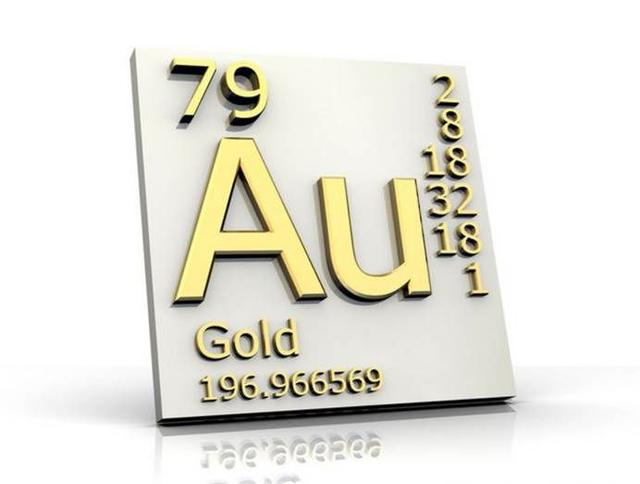
(Summary description)Gold has been considered a valuable precious metal since ancient times, and its unique chemical and physical properties have led to its extensive use in various fields. It serves as both a special reserve and investment currency, dominates the jewelry industry, and plays a crucial role in modern industries such as telecommunications, aerospace, and aviation. In the field of electronic device manufacturing, gold is highly regarded for its excellent conductivity. Gold's conductivity is not only superior to common conductive metals like copper and silver but also exhibits excellent stability in extreme environments such as high temperatures, high pressures, and low temperatures. Therefore, gold finds wide applications in semiconductors and electronic components.
Application of Gold in High-end Manufacturing-Electronic Semiconductor
(Summary description)Gold has been considered a valuable precious metal since ancient times, and its unique chemical and physical properties have led to its extensive use in various fields. It serves as both a special reserve and investment currency, dominates the jewelry industry, and plays a crucial role in modern industries such as telecommunications, aerospace, and aviation. In the field of electronic device manufacturing, gold is highly regarded for its excellent conductivity. Gold's conductivity is not only superior to common conductive metals like copper and silver but also exhibits excellent stability in extreme environments such as high temperatures, high pressures, and low temperatures. Therefore, gold finds wide applications in semiconductors and electronic components.
- Categories:Application Technology
- Author:UMM
- Origin:
- Time of issue:2023-12-01 09:15
- Views:0
Gold has been considered a valuable precious metal since ancient times, and its unique chemical and physical properties have led to its extensive use in various fields. It serves as both a special reserve and investment currency, dominates the jewelry industry, and plays a crucial role in modern industries such as telecommunications, aerospace, and aviation. In the field of electronic device manufacturing, gold is highly regarded for its excellent conductivity. Gold's conductivity is not only superior to common conductive metals like copper and silver but also exhibits excellent stability in extreme environments such as high temperatures, high pressures, and low temperatures. Therefore, gold finds wide applications in semiconductors and electronic components.
Gold is primarily used in the form of electroplating chemicals, gold bonding wire, and sputtering targets in electronic semiconductors. In electronic products, the most significant use of gold is as electroplated coatings for connectors and contact points. Additionally, gold is used in gold bonding wires within semiconductor packaging. Other applications include solderable coatings for hybrid circuits, printed circuit boards, and components, metal layers on gold-based solder or semiconductors, and conductor traces and contact pads.
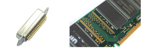
1、Connectors and Contacts
Connectors and contacts can be made from a variety of materials, and the choice of the appropriate material depends on several factors, including current, voltage, contact force, wear, micro-motion (due to vibration and thermal cycling), environmental conditions (temperature, corrosive gases, etc.), material cost, and more.
Gold is used for connectors and contacts primarily because it possesses excellent corrosion resistance and high conductivity. When alloyed with small amounts of nickel or cobalt, it also exhibits improved wear resistance. For applications with low voltage, low current, and low contact force, gold is the best material.
An important criterion for connector and contact materials is their susceptibility to fretting corrosion. Susceptibility is often determined using standard electrode potential data. Table 1 provides electrode potential values for various metals. Generally, larger positive values indicate good corrosion resistance, while larger negative values indicate higher reactivity. However, the actual situation is not always so straightforward, as some metals like copper and iron can form oxides such as copper oxide and aluminum oxide over time. These oxides can lead to wire breakage and poor contacts in integrated circuits.
|
Metal |
Standard Electrode Potential (Volts) |
Evaluation |
|
Gold |
Au+→Au:+1.68 |
Very inert, resistant to oxidation and corrosion. |
|
Palladium |
Pd2+→Pd:+0.83 |
Lower corrosion resistance and oxidation resistance compared to gold. |
|
Silver |
Ag+→Ag:+0.80 |
Exhibits good oxidation resistance and corrosion resistance but can be susceptible to attack by sulfides and chlorides. |
|
Copper |
Cu2+→Cu:+0.34 |
Prone to oxidation in the presence of air and susceptible to corrosion in humid conditions. |
|
Tin |
Sn2+→Sn:-0.136 |
Forms a thin, protective, inert oxide layer. Tin is relatively soft and can be easily damaged. |
|
Nickel |
Ni2+→Ni:-0.23 |
Forms a thin but strong and protective oxide layer, preventing further oxidation. It also acts as a good electrical insulator. |
|
Aluminum |
Al3+→Al:-1.7 |
Aluminum is highly reactive but quickly forms a thin, protective, inert oxide layer with strong protective properties. |
Table 1: Standard Electrode Potentials of Metals
The choice of the final material for connectors or contacts often involves a trade-off between performance and cost. Table 2 provides a summary of the pros and cons of commonly used materials for low connectors and contacts, comparing them to gold. The actual contact area for closed connectors or a pair of contacts is typically very small compared to the surface dimensions because contact occurs only at a few very small locations. This increases the resistance between the contacts, leading to the generation of heat as current passes through. Increasing contact pressure enlarges the contact area, thereby reducing resistance. Voltage and contact pressure both influence localized heating, leading to surface oxidation or melting. Arcing can also occur. All of these factors can affect the lifespan of the contacts. Oxidation or corrosion may affect alloying elements added to gold, but these elements are used to modify its properties, such as hardness or dissolution rate.
|
Gold |
Pure gold is relatively soft, so hard gold is often used. Pure gold is resistant to corrosion or oxidation, but alloying elements may be susceptible. Hard gold alloyed with 0.4% Co forms insulating oxides when used at 200°C. Gold is typically electroplated onto nickel. |
|
Silver |
Due to its low cost, silver is commonly used as an alternative to gold, but it can lose its luster easily when affected by trace amounts of sulfides, and it has poor wear resistance. |
|
Tin |
Tin is cheaper than silver but is susceptible to corrosion. Initial contact resistance is higher than that of gold, and once oxidation or corrosion occurs, contact resistance deteriorates. |
|
Palladium/Nickel |
Initially introduced as a low-cost alternative to gold but now palladium is also relatively expensive. Palladium has excellent wear resistance but is susceptible to oxidation, corrosion, and forming insulation films at high temperatures. Typically, palladium is electroplated onto nickel. |
|
Gold/Palladium Nickel |
Thin gold flash is used on palladium to reduce oxidation and corrosion. |
|
Gold Alloys |
Gold alloys offer good corrosion resistance and are used for electrical contacts. They reduce the cost of gold but do not have the conductivity of pure gold. |
|
Copper and its Alloys |
Clean, non-oxidized copper has excellent conductivity but is quickly oxidized and corroded if insulated oxide coatings are present. It is often used in applications with high contact force and power transmission. |
Table 2: Material Comparison for Connectors and Contacts
With the development of the Internet of Things (IoT), an increasing number of devices are being connected to provide instant access to information and data. In other words, the effectiveness and reliability of any electrical device depend largely on the quality of the connection, especially the plating used on connectors or contacts. Even tiny variations in contact resistance can affect product performance, particularly in low-voltage signal transmission applications. Therefore, in critical applications that require highly reliable real-time signal transmission, such as life-safety sensors or autonomous vehicles, gold is currently the only medium that can achieve this. Compared to other metals, gold does not form sulfides or lose its luster under normal conditions, making it a more viable choice for connectors and contacts in the electronic semiconductor industry.
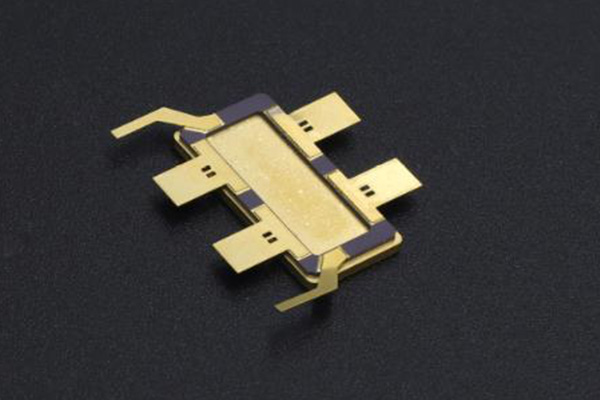
2、Bonding Wire for Packaging
Bonding wire, as one of the four fundamental key materials in the field of microelectronics packaging (the other three being chips, lead frames/substrates, and encapsulants), serves as the inner wire for electrical interconnection in chip-to-lead frame bonding. It plays a crucial role in connecting semiconductor chips to external circuits for current transmission and signal interconnection, and it is widely used in the packaging of semiconductor discrete devices and integrated circuits. Currently, there are four types of bonding wire products commonly used in the market: gold bonding wire, copper bonding wire, silver bonding wire, and aluminum bonding wire.

Compared to copper and silver, although gold is more expensive, gold bonding wires have excellent ductility, good conductivity, fast wire bonding speed, and high reliability. Therefore, they are the earliest and most widely used type of bonding wire. Typically, they are 2mm long, 25μm thick, and each wire uses only about 20 nanograms of gold. With the increasing demand for integrated circuits, some integrated circuits may have over 200 wire bonding connections, leading to a continuous increase in the amount of gold used for wire bonding. In 2022, semiconductor bonding wire demand in China increased to 36.01 billion meters, with gold bonding wire demand reaching 6.23 billion meters.
3、Gold Solder
In semiconductor power devices, chips generate a significant amount of heat, requiring effective heat dissipation to prevent damage. Typically, any device with a power output exceeding 5 watts needs a good thermal pathway for heat dissipation. This can be achieved by bonding the chip to the package using solder alloys.
As the market demands the development of high-performance power devices, there are higher expectations for semiconductor device package solders. Factors to consider include the solder's printability (dispensing), the reliability of soldering, the cleanability of flux residue, compatibility with flux residue and encapsulation materials, and more. Additionally, the characteristics of power devices, such as high current, high heat generation, and ultra-high power, must be taken into account.The trend in power devices towards smaller grain area can offer advantages in performance and cost but may pose challenges in heat dissipation. Meanwhile, the development towards higher voltages and lower losses demands solder layers with reduced void content.
Currently, commonly used solder alloys in the market include the Gold-Tin series represented by Au80Sn20, the Tin-Silver-Copper series represented by SAC305, the Tin-Silver-Indium-Bismuth series represented by Sn88Ag3.5In8Bi0.5, the Tin-Antimony series represented by SnSb5 and SnSb10, the Tin-Bismuth series represented by Sn42Bi58, and indium-based solder alloys.
Indium-based solder alloys are one of the most commonly used solder materials for high-power semiconductor laser packaging. However, they are prone to electromigration and thermomigration issues at high currents, which can affect the stability of semiconductor lasers. Lasers packaged with indium-based solder materials have a significantly shorter lifespan compared to devices packaged with gold-tin solder materials, and they may experience sudden performance degradation during use. The use of indium-free packaging technology can overcome the electromigration issues associated with indium-based solder layers. In the selection of indium-free solder materials, gold-tin solder has become an important solder material in packaging due to its stable device performance.
Eutectic tin/lead solder can form good bonds and has relative flexibility. However, it is not suitable if component leads are soldered to PCBs or other parts using standard solder. Additionally, as the integration density of integrated circuits increases, IC pins become more densely packed. The vertical tin-spraying process can make it challenging to achieve flat pads, which, in turn, makes surface mount technology (SMT) placement difficult. Furthermore, tin-plated boards have a short shelf life. While high-melting-point solder with a high lead content can be used, it may result in porous and gapped joints, leading to stress and hotspots at the junctions.
Table 3 lists the characteristics of commonly used chip connection solders. A comparison shows that gold solder has better thermal conductivity and a higher melting point than tin or lead solder. It is the only solder within the melting point range of 280-360°C that can replace high-melting-point lead-based alloys. Compared to high-lead-content alloys, gold alloy solder offers better resistance to thermal fatigue. Moreover, a typical integrated circuit uses only 2-3 milligrams of gold, which falls within an acceptable cost range. It can be used for chip-to-circuit substrate connections as well as high-reliability circuit hermetic sealing. For example, in the case of laser diodes used in internet communications, 80Au20Sn is employed as the sealing and chip connection solder. It's clear that gold alloy solder has wide-ranging applications in the semiconductor electronics industry.
|
Alloy |
Thermal Conductivity (W/mK) |
Melting Temperature (°C) |
|
63%Sn-37%Pb |
51 |
183 |
|
99%Sn-1%Sb |
29 |
235 |
|
88Pb%-10%Sn-2%Ag |
27 |
268-290 |
|
90%Pb-5%Sn-5%Ag |
26 |
292 |
|
Gold-Tin (Au-Sn) |
57 |
280 |
|
Gold-Silicon (Au-Si) |
27 |
363 |
|
Gold-Germanium (Au-Ge) |
44 |
361 |
Table 3 Solder Paste Performance
4、Solderable Coating
After printed circuit boards (PCBs) are manufactured, the copper circuits on them quickly oxidize, making it difficult for electronic soldering flux to wet the surface. Therefore, a protective layer is needed on the PCB to protect it during storage. The most commonly used are chemical nickel-gold and immersion gold. Using gold is more expensive than some alternatives, but gold offers superior performance. For instance, using Organic Solderability Preservatives (OSP), while cost-effective, makes the protective coating very susceptible to damage from fingerprints and light abrasion. There are also tin and silver coatings, which are less susceptible to damage compared to organic solderability preservatives but are more prone to losing luster or corroding compared to nickel/gold. In contrast, gold can form a very flat coating surface, making it suitable for directly soldering bare chips onto the PCB, and it easily wets with liquid solder. The thickness of gold typically used is 0.08μm, so very little gold is used per PCB, and the cost remains within an acceptable range. During soldering, this very small amount of gold dissolves into the solder and remains in the solution, thus not affecting the reliability of the connection. Solder forms a strong bond with nickel, and nickel dissolves in liquid solder much slower than gold or copper. Nickel cannot be used alone without a thin immersion gold layer since it oxidizes when exposed to the air, forming a very stable oxide that prevents solder from wetting the surface. Highly corrosive solder flux can alleviate this problem, but it's not suitable for electronic circuits.
Electromigration is a process that can affect printed circuit boards, hybrid printed circuit boards, and certain electronic components under certain conditions, characterized by the filament-like growth of metal between two conductors. Conditions that can lead to electromigration include high humidity, voltage, and the presence of ionic materials such as solder flux residues. Most metals can experience electromigration under certain conditions, such as silver and aluminum conductors. However, electromigration in gold is very rare and only occurs in the presence of chloride ions.
|
Characteristics |
HASL |
OSP |
Chemical Nickel/Gold |
Electroless Nickel/Electrolytic Gold |
Immersion Silver |
Immersion Tin |
|
Solder Joint Reliability |
Good |
Good |
BGA "Black Pad" and Solder Joint Brittleness Issues |
Gold Brittleness Issues |
Good |
Good |
|
Test Point Detection |
Good |
Poor |
Good |
Good |
Good |
Good |
|
Exposed Copper After Assembly |
No |
Yes |
No |
No |
No |
No |
|
Switch/Contact |
No |
No |
Yes |
Yes |
Yes |
No |
|
Waste Disposal and PCB Manufacturing Safety |
Poor |
Good |
Fair |
Fair |
Good |
Good |
|
Surface Coating Thickness Control |
Thickness Control Issues |
Good |
Good |
Thickness Control Issues |
Good |
Good |
|
Cost |
1 |
1 |
1.1-1.3 |
1.2-1.5 |
1 |
1 |
Table 4: Coating Material Performance Comparison
-
Gold Plating by Sputtering
As the electronics industry has evolved from vacuum tubes to semiconductor integrated circuits and very-large-scale integrated circuits, it has brought about revolutionary impacts on various aspects of human society. High-purity gold sputtering targets, as key source materials for the preparation of electrode thin films in various semiconductor wafers and integrated circuits in the electronics industry, have become crucial. As electronic chips continue to develop towards being lighter, thinner, smaller, and higher in density, there is relatively less tolerance for defects. Furthermore, with the increasing density of integrated circuit devices, the area of individual chips has become smaller. Defects that would not have affected yield in the past have now become critical issues. Therefore, higher demands are placed on the purity, grain size, uniformity, and stability of the microstructure of high-purity gold targets.
In the field of electronic thin films, gold thin films are primarily obtained through a process called magnetron sputtering. The sputtering principle of gold targets is depicted in the diagram below:
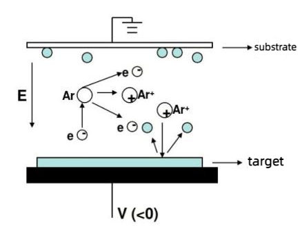
FIG. 2 Sputtering principle diagram of gold target
As the cathode, the gold target material undergoes collisions with argon atoms in the sputtering chamber when electrons are accelerated by the applied voltage, leading to the ionization of a significant number of Ar+ ions and electrons. Electrons travel towards the substrate, while the Ar+ ions, accelerated by the electric field, bombard the gold target and sputter a large number of gold atoms. These neutral gold atoms deposit on the substrate to form a film.
During the sputtering process, due to the presence of a magnetic field, electrons are subjected to the Lorentz force from the magnetic field, confining them to the plasma region near the target surface, where they move in circular paths around the target surface. Gold exhibits a magnetic susceptibility of only (-0.141 to -0.143) × 10^-6 cm^3/g in the temperature range of 7.8-975K, making it an excellent conductor with good high-temperature oxidation resistance.
To reduce costs and save gold consumption, the design of the gold target material's structure is primarily based on the magnetic field structure of the magnetron sputtering equipment's cathode. The shape of the target material must be compatible with the sputtering equipment in use.

High-purity gold sputtering targets of different sizes
Gold can be deposited onto various substrates, including metals, ceramics, and plastics, using a variety of vacuum coating techniques. In sputtering technology, gold is used in the form of a "target." Gold is an excellent optical reflector with outstanding corrosion resistance and resistance to fading. During the coating process, high-energy ions eject gold atoms from the surface, which then deposit onto the substrate.
As a cathode source material in the sputtering process, the target material needs to be securely fixed to the cathode of the sputtering equipment. Additionally, it needs to be conductive during the sputtering process and may generate some heat. Therefore, most target materials require a backing material with adequate strength and good heat dissipation properties, such as aluminum or copper, to provide structural support, electrical conductivity, and heat conduction. The connection between the target material and the backing material is called bonding and is a crucial step in the sputtering target preparation process. The quality of bonding directly impacts the sputtering process and the quality of the product film. Currently, common bonding methods for gold targets include brazing and composite embedding.
As the electronic semiconductor industry continues to advance in equipment design and experiences growing demands in the future, highly precise chip manufacturing processes are needed. This is where precious metals like gold come into play. Although the demand for gold in these miniature electronic components is relatively small, the absence of gold can significantly impact the performance of chips and end devices. Therefore, this ancient precious metal continues to demonstrate its strong vitality and potential in modern semiconductor technology.
From bonding wires to polishing processes and into the realm of miniaturization, gold plays a critical role throughout. With the ongoing progress in semiconductor technology, we anticipate that gold's applications in this field will become even more widespread and profound.
Reference:
-
Paul Goodman, Current and Future uses of gold in electronics, Gold bulletin
-
Wu W H., Study on the preparation of high purity gold by centrifugal extraction, Gold,2018
-
Zhang Q, Manufacture, application and trends of gold-base supptering target alloys, Materials review,2014
-
He J J, Application and fabrication method of high purity precious metals sputtering targets used in semiconductor, Precious metals,2013
Scan the QR code to read on your phone
Hot Technology Ranking

2022-10-20

Scan the QR code and follow the official account
Products
Precious metal functional materials
High-quality optoelectronic materials/high-purity targets
Refractory metals and their alloys
Special alloy/special steel
Spherical | Nano powder
Biomedical/3D printing products
Compound
Rare metals and their alloys
Rare metals and their alloysRare Metal Concept Cultural/Art/Collectible
Nuclear energy Nuclear power Nuclear industry
High temperature heat container
Microelectronics industry Chip thermal sink
Semiconductor equipment MOCVD thermal field
High efficiency & long life Wire for wire cutting
Medical equipment Medical instruments
Artificial bone joint Bioimplantation
Rare metal cultural & creative art collection Precious metal
Plasma|Special Welding Electrode
Ultra Minor Metals Ltd (UMM) all rights reserved 湘ICP备17001881号 by:www.300.cnchangsha