


Application Technology
Understand cutting-edge application technology
Application Technology
What are the characteristics of high-quality sputtering targets?
- Categories:Application Technology
- Author:
- Origin:
- Time of issue:2023-04-19 14:30
- Views:0
(Summary description)PVD (Physical Vapor Deposition) technology is one of the main technologies for preparing thin film materials. Under vacuum conditions, physical methods are used to vaporize a material into gaseous atoms, molecules, or partially ionize it into ions, and through a low-pressure gas (or plasma) process, thin film materials with special functions such as transparency enhancement, reflection, protective conductivity, magnetic conductivity, insulation, corrosion resistance, oxidation resistance, radiation protection, and decoration are deposited on the surface of the substrate material. T
What are the characteristics of high-quality sputtering targets?
(Summary description)PVD (Physical Vapor Deposition) technology is one of the main technologies for preparing thin film materials. Under vacuum conditions, physical methods are used to vaporize a material into gaseous atoms, molecules, or partially ionize it into ions, and through a low-pressure gas (or plasma) process, thin film materials with special functions such as transparency enhancement, reflection, protective conductivity, magnetic conductivity, insulation, corrosion resistance, oxidation resistance, radiation protection, and decoration are deposited on the surface of the substrate material. T
- Categories:Application Technology
- Author:
- Origin:
- Time of issue:2023-04-19 14:30
- Views:0
PVD (Physical Vapor Deposition) technology is one of the main technologies for preparing thin film materials. Under vacuum conditions, physical methods are used to vaporize a material into gaseous atoms, molecules, or partially ionize it into ions, and through a low-pressure gas (or plasma) process, thin film materials with special functions such as transparency enhancement, reflection, protective conductivity, magnetic conductivity, insulation, corrosion resistance, oxidation resistance, radiation protection, and decoration are deposited on the surface of the substrate material. The material used to prepare thin film materials is referred to as PVD coating materials. Currently, the two most mainstream PVD coating materials are sputtering target materials and vapor deposition materials. The sputtering coating process has good repeatability and controllable film thickness, and can obtain thin films with uniform thickness on large area substrate materials. The prepared thin films have the advantages of high purity, good compactness, and strong adhesion to substrate materials, and have become one of the main technologies for preparing thin film materials. Various types of sputtering thin film materials have been widely used, so the demand for sputtering targets, a functional material with high added value, has increased year by year. Sputtered targets have also become the PVD coating material with the largest market application. This article focuses on the general characteristics of sputtering targets and the advantages of high-quality sputtering targets.
1.General characteristics of sputtering targets
Sputtering target material is one of the main materials for preparing thin films, which has the characteristics of high purity, high density, multi-component, uniform grain size, and generally consists of a target blank and a back plate. Target blank is the core part of sputtering target material, which is the target material bombarded by high-speed ion beam. After the target is impacted by ions, its surface atoms are sputtered out and deposited on the substrate to form an electronic thin film. Due to the fact that the target material needs to complete the sputtering process in a high voltage and high vacuum machine environment, the target blank needs to be bonded to the back plate through different welding processes. The back plate mainly serves to fix the sputtering target blank, and needs to have good electrical and thermal conductivity. Sputtered targets are mainly used in integrated circuits, flat panel displays, solar cells, recording media, smart glass, etc. Generally, high requirements are placed on the purity and stability of the targets. With the rapid development of iterative upgrading of electronic processes and thin film technology, the market demand for high-quality sputtering targets is rapidly increasing at an annual rate of nearly 15%. The obvious development trend of high-quality sputtering targets is: high purity/ultra high purity metal above 4N level, high sputtering rate, controllable grain/orientation, and large size.
2. Varieties and classification of sputtering target materials
(1) According to the chemical composition and material of the target, the sputtering target can be divided into metal/non-metallic single material targets, alloy targets, ceramic/compound targets, and so on.
(2) According to the shape of the target material, there are mainly long targets, square targets, round targets, and tube targets.
(3) Classified by application field, there are mainly semiconductor targets, flat panel display targets, solar cell targets, and so on.
3. Main application fields and technical requirements of sputtering target materials
High purity sputtering targets are mainly used in four fields: flat panel display, information storage, solar cells, and chips, accounting for 94% of the total. The chip industry, that is, the semiconductor industry, has the most stringent and demanding requirements for target materials. Copper, aluminum, molybdenum, and ITO targets are the most common and widely used targets.
1)Chip field
"Chip" is the most advanced application field of target materials and the targets are mainly used in the two stages of "wafer manufacturing" and "chip packaging". It is mainly used for metal splash plating in the wafer manufacturing process, and commonly used as the coating of chip bonding lines in the chip packaging process. Chip target is a key raw material for manufacturing integrated circuits, and also the target with the highest technical requirements. It is necessary to ensure ultra-high purity, high-precision dimensions, and high integration. Therefore, the materials selected are mostly high purity copper, high purity aluminum, high purity titanium, high purity tantalum, high purity tungsten, copper manganese alloy, etc., and integrated circuit chips generally require a target purity of more than 5N5. The dielectric layer, conductor layer, and protective layer also need to use a target of purity of more than 5N for sputtering coating. Advanced processes require higher purity metals.
The purpose of selecting metal sputtering targets for semiconductor chips is to create metal wires on the chip that transmit information. Firstly, high-speed ion currents are used to bombard the surfaces of different types of metal sputtering targets under high vacuum conditions, so that atoms on the surfaces of various target materials are deposited layer by layer on the surface of the semiconductor chip. Then, through a special processing process, the metal film deposited on the surface of the chip is etched into nanoscale metal wires, connecting hundreds of millions of micro transistors inside the chip, so as to transmit signals.
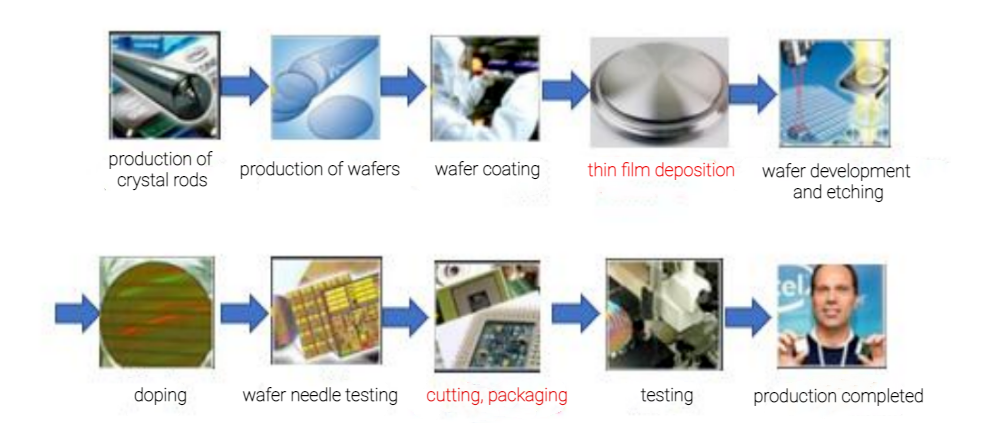
Application of target materials in chip production process
With the rapid development of information technology, the requirements for integrated circuits are becoming higher and higher, and the size of unit devices in circuits is constantly shrinking, with the size of components ranging from millimeter to micrometer to nanometer. The interior of each unit device is composed of a substrate, an insulating layer, a dielectric layer, a conductive layer, and a protective layer. The dielectric layer, the conductive layer, and the protective layer are sputtered and coated with a target material with a purity of more than 5N, which is one of the cores of the preparation of integrated circuits. The target materials for coating in the field of integrated circuits mainly include aluminum targets, copper targets, titanium targets, tantalum targets, and tungsten targets. The purity requirement is generally above 5N (99.999%), while the purity of aluminum targets is often above 5N5 (99.9995%). Therefore, the price of chip targets is relatively the most expensive.
The chip target mainly consists of copper, tantalum, aluminum, and titanium to construct the interconnection conductors in integrated circuits. The advanced technology of "copper and tantalum" can reduce power consumption and improve computing speed. "Aluminum and titanium" above 110nm can ensure the reliability and anti-interference performance of chips, such as flash memory chips, processor chips, power management, and sensor chips. Currently, in addition to using "copper" as a conductor and "tantalum" as a barrier layer in 14nm and 28nm wafer technology nodes, "titanium" is also widely used as the main material for dielectric metal gate technology with high dielectric constant and "aluminum" as the main material for wafer bonding pad processes. Overall, the use of chips has become increasingly widespread, and the demand for chips in the market has shown an explosive growth, which will also drive the use of aluminum, titanium, tantalum, and copper, the four mainstream thin film metal materials in the industry.
Multi variety, large size, and 5N level high purity are the future development trends of chip target technology. With the gradual application of large size wafers in chips, the development of target materials towards large size is also being promoted. At the same time, as the size increases, the difficulty of controlling the grain orientation of the target increases exponentially. During the sputtering process, atoms in the sputtering target are easily sputtered out along a specific direction, and the crystal orientation of the sputtering target can affect the sputtering rate and the uniformity of the sputtering film, ultimately determining the quality of the product. Therefore, obtaining a target structure with a certain crystal orientation is crucial. However, in order to obtain a certain crystal orientation inside the sputtering target, there is a greater difficulty. According to the structural characteristics of the sputtering target, different molding methods need to be adopted, and repeated plastic deformation and heat treatment processes need to be carried out to control it.
When the sputtering target is bombarded by a high speed energy ion beam, the gas existing in the internal voids of the sputtering target is suddenly released, resulting in the splashing of large-sized sputtering target particles. The appearance of these particles can reduce the quality of the sputtering film and even lead to product scrapping. For example, in the process of large-scale integrated circuit manufacturing, the allowable number of particles per 150mm diameter silicon wafer must be less than 30. Therefore, in order to meet the needs of semiconductor nanoscale processes with higher accuracy and smaller dimensions, the required purity of sputtering target materials continues to rise, even reaching 99.9999% (6N) purity or above.
2)Flat panel display field
Flat panel displays mainly include liquid crystal displays (LCD), plasma displays (PDP), field luminescent display (EL), field emission displays (FEDs), organic light emitting diode displays (OLEDs), and touch panel (TP) display products developed on the basis of LCD. Among them, the market applications are mainly liquid crystal displays. The raw materials for flat panel display targets include high-purity aluminum, copper, molybdenum, and other materials, as well as indium tin oxide (ITO targets). The technical requirements for flat panel display targets are also relatively high, requiring high material purity, large area, and good tissue uniformity. Generally, aluminum targets with a purity of more than 5N are used. Coating is a fundamental part of the modern flat panel display industry. In order to ensure the uniformity of large area film layers, improve productivity, and reduce costs, almost all types of flat panel display devices use a large number of coating materials to form various functional films. The PVD coating materials used are mainly sputtering targets. Many properties of flat panel displays, such as resolution, light transmittance, and so on, are closely related to the performance of sputtering films.
The flat panel display industry mainly uses PVD coating materials in the production of display panels and touch screen panels. In the production process of flat panel display panels, the glass substrate undergoes multiple sputtering and coating processes to form ITO glass, which is then coated, processed and assembled for the production of LCD panels, PDP panels, and OLED panels. For the production of touch screens, ITO glass needs to be processed, coated to form electrodes, and then assembled with protective screens and other components. In addition, in order to achieve the anti-reflection, shadow elimination, and other functions of flat panel display products, it is also possible to increase the coating of corresponding film layers in the coating process.
4.Distribution of sputtering target industry chain and demand trend for high-quality sputtering target materials
The sputtering target industry chain is basically distributed in a pyramid, mainly including four links: metal purification, target manufacturing, sputtering coating, and terminal application. Among them, metal purification and target manufacturing are the most important basic links of raw materials in the electronic industry, while sputtering coating is the most technically demanding link in the entire industrial chain, because the quality of sputtering films has an important impact on the quality of downstream products. Terminal application is the largest sector in the entire industry chain, such as semiconductor chips, flat panel displays, solar cells, and other fields mentioned above.
The upstream metal purification mainly starts from ordinary industrial grade raw materials. Generally, industrial grade metals can achieve a purity of 99.8%, while sputtering targets need to achieve at least 99.95% purity. Semiconductor grade high-quality sputtering targets used for chip manufacturing even require a purity of 99.99~99.9999% (4N~6N). In the target manufacturing process, it is first necessary to conduct process design based on the performance requirements of downstream application fields, then conduct repeated plastic deformation and heat treatment to control key indicators such as grain size and orientation, and then undergo water cutting, mechanical processing, metallization, ultrasonic testing, ultrasonic cleaning, and other processes. The manufacturing process of sputtering target material is delicate and diverse, and the process flow management and manufacturing process level will directly affect the quality and yield of sputtering target material. This link is the highest demand for production equipment and technology in the sputtering target industry chain, and the quality of sputtering films has an important impact on the quality of downstream film products.
During the sputtering coating process, the sputtering target needs to be installed in a machine to complete the sputtering reaction. The sputtering machine has strong specificity and high precision, and the market has long been monopolized by multinational groups in the United States and Japan. The main equipment suppliers include well-known enterprises in the industry such as AMAT (the United States), ULVAC (Japan), ANELVA (Japan), Varian (the United States), and ULVAC (Japan).
Scan the QR code to read on your phone
Hot Technology Ranking

2022-10-20

Scan the QR code and follow the official account
Products
Precious metal functional materials
High-quality optoelectronic materials/high-purity targets
Refractory metals and their alloys
Special alloy/special steel
Spherical | Nano powder
Biomedical/3D printing products
Compound
Rare metals and their alloys
Rare metals and their alloysRare Metal Concept Cultural/Art/Collectible
Nuclear energy Nuclear power Nuclear industry
High temperature heat container
Microelectronics industry Chip thermal sink
Semiconductor equipment MOCVD thermal field
High efficiency & long life Wire for wire cutting
Medical equipment Medical instruments
Artificial bone joint Bioimplantation
Rare metal cultural & creative art collection Precious metal
Plasma|Special Welding Electrode
Ultra Minor Metals Ltd (UMM) all rights reserved 湘ICP备17001881号 by:www.300.cnchangsha