


Application Technology
Understand cutting-edge application technology
Application Technology
Overview of Chemical Vapor Deposition (CVD) Coating
- Categories:Application Technology
- Author:UMM
- Origin:
- Time of issue:2023-07-26 09:09
- Views:0
(Summary description)With the continuous improvement in the requirements of aerospace, nuclear industry, semiconductors, and other fields for semiconductor devices, integrated circuits, high-field and small-sized superconducting materials, and crystal growth products, chemical vapor deposition technology has a broad market application prospect as an essential method for material preparation and effective surface modification. Some researchers predict that CVD will focus on reducing harmful by-products and increasing industrial-scale production in the future. Additionally, the development of lower-temperature CVD processes, more precise control over CVD processes, thick film deposition techniques, novel film materials, and new material synthesis technologies will be the major areas of research in the future.
Overview of Chemical Vapor Deposition (CVD) Coating
(Summary description)With the continuous improvement in the requirements of aerospace, nuclear industry, semiconductors, and other fields for semiconductor devices, integrated circuits, high-field and small-sized superconducting materials, and crystal growth products, chemical vapor deposition technology has a broad market application prospect as an essential method for material preparation and effective surface modification. Some researchers predict that CVD will focus on reducing harmful by-products and increasing industrial-scale production in the future. Additionally, the development of lower-temperature CVD processes, more precise control over CVD processes, thick film deposition techniques, novel film materials, and new material synthesis technologies will be the major areas of research in the future.
- Categories:Application Technology
- Author:UMM
- Origin:
- Time of issue:2023-07-26 09:09
- Views:0
1.Introduction to Chemical Vapor Deposition (CVD)
Modern methods for thin film fabrication include Physical Vapor Deposition (PVD), Chemical Vapor Deposition (CVD), and Plasma Chemical Vapor Deposition (PCVD). Among these, Chemical Vapor Deposition (CVD) is a process where reactants undergo chemical reactions under specific atmospheric conditions, leading to the deposition of solid materials on a heated solid substrate. This technique is used to produce various solid materials and has become the most widely applied method due to its matured research and technological development.
CVD is extensively utilized in purifying substances and preparing a wide range of single-crystal, polycrystalline, or amorphous inorganic thin film materials.
2.Principles of Chemical Vapor Deposition (CVD)
The principle process of CVD involves introducing two or more gaseous precursor materials into a reaction chamber, where they undergo a chemical reaction to form a new material that deposits onto the surface of a substrate. The reaction materials are first heated to a certain temperature, reaching a sufficiently high vapor pressure. Argon or hydrogen gas is used as a carrier gas and introduced into the reactor. The material to be coated is either coated on a metal wire, suspended in the reactor, placed on a flat surface, submerged in a fluidized bed of powder, or is already a particle in the fluidized bed.
Inside the chemical reactor, the products of the chemical reaction deposit onto the surface of the substrate, while waste gases, such as HCl or HF, are directed to alkaline absorption or traps. Apart from the desired solid deposit, all other reaction products must have low enough saturation vapor pressure to ensure that they remain on the heated substrate throughout the entire reaction and deposition process.
The principle process can be summarized in four main reaction stages:
1. Diffusion of the reaction gas towards the substrate surface.
2. Adsorption of the reaction gas onto the substrate surface.
3. Chemical reaction occurring on the material surface.
4. Detachment of gaseous by-products from the material surface.

Figure 1: Basic Process Flow of Chemical Vapor Deposition, CVD
The chemical reaction selected should typically meet the following criteria:
1. The reactants should preferably be gaseous at room temperature or moderately high temperatures, with high vapor pressure and high purity.
2. The deposition reaction should form the desired material deposit layer.
3. The reaction should be easily controllable at the deposition temperature, requiring the reactants to have sufficiently high vapor pressure.

Figure 2: Schematic diagram of CVD reaction system
3.Characteristics of Chemical Vapor Deposition (CVD)
1. Diverse Types of Deposits: CVD can deposit various types of films, including metal films, non-metal films, multi-component alloy films as required, as well as ceramic or compound layers.'
2. Deposition under Atmospheric or Vacuum Conditions: CVD can be carried out under atmospheric pressure or negative pressure (vacuum). Typically, films deposited under vacuum conditions exhibit better quality.
3. Adjustable Chemical Composition: The chemical composition of the coating can be adjusted according to changes in the gas phase composition, allowing for gradient deposition or mixed coatings.
4. Suitable for Complex Substrates: CVD is suitable for coating on complex-shaped substrates and particulate materials. It is well-suited for coating various intricate workpieces with features such as grooves, slots, holes, and even blind holes. The film thickness is generally uniform, the film quality is stable, and it is easily adaptable for mass production.
5. Columnar Crystal Structure: The deposited layer typically has a columnar crystal structure, making it less flexible. However, various techniques can be used to disturb the chemical reaction in the gas phase to improve its structure. Research has shown that using CVD technology to deposit highly wear-resistant carbides, nitrides, carbonitrides, borides, and diamond films on the substrate surface can provide wear resistance over 100 times higher than that of hard alloys.
However, Chemical Vapor Deposition (CVD) also has some drawbacks:
1. Relatively Low Deposition Rate: The deposition rate of CVD is generally in the range of a few to a few hundred nm/min, which is not as high as techniques like evaporation and ion sputtering, and may even be lower than sputter coating.
2. Safety Concerns: In many cases, the reactants involved in the deposition process and the residual gases after the reaction can be flammable, explosive, or toxic. Therefore, measures need to be taken to prevent environmental pollution. Additionally, the equipment used in CVD often requires corrosion resistance.
3. Difficulty with Localized Deposition: Deposition of films on specific areas or surfaces of a substrate can be challenging in CVD, making it less convenient than PVD techniques.
4. High Workpiece Temperature: Even with the implementation of new techniques, the workpiece temperature during CVD film formation remains higher than in PVD techniques, limiting certain applications.
4.Classification of Chemical Vapor Deposition (CVD)
1. According to Temperature:
Low-temperature CVD (200 ~ 500°C)
Medium-temperature CVD (500 ~ 1000°C)
High-temperature CVD (1000 ~ 1300°C)
2. According to Pressure:
Atmospheric Pressure CVD (APCVD): CVD conducted at atmospheric pressure. This was the original method used for CVD. It requires a simple system, has fast reaction rates, and high deposition rates, making it suitable for depositing thick films on substrates. However, it may have lower uniformity, so it is generally used for thick film deposition.
Low-Pressure CVD (LPCVD): CVD performed at lower pressures. LPCVD is used not only for silicon epitaxial layers but also for depositing various amorphous passivation films and polycrystalline silicon thin films. It is an important thin-film deposition technique.
3. According to the reaction chamber wall temperature: there are hot-wall CVD and cold-wall CVD.
Hot-wall CVD: A method where the wall temperature is higher than the wafer temperature. Typically, an external electric resistance heating method is used outside the reaction chamber to heat the wafer through the chamber wall.
Cold-wall CVD: A method where the wall temperature is lower than the wafer temperature. It can be achieved by using radio frequency induction or resistance heating within the reaction chamber to heat the substrate.
4. According to the activation method of the reaction: there are plasma activation (PECVD), thermal activation, and ultraviolet light activation, etc.
Plasma-enhanced chemical vapor deposition (PECVD): A gas-phase deposition technique that uses high-frequency plasma to drive the process. It combines physical processes involving radio frequency glow discharge with chemical reactions. This gas-phase deposition method allows the deposition of thin films at
very low substrate temperatures. For example, SiO2 can be deposited on aluminum (Al) at low temperatures. In practice, plasma-enhanced chemical vapor deposition is mainly used for depositing insulating layers.
5.New Chemical Vapor Deposition (CVD) Techniques
1. Metal-Organic Chemical Vapor Deposition (MOCVD)
MOCVD is a method of chemical vapor deposition that utilizes metal-organic compounds, which are easily decomposable and volatile at low temperatures, as source materials. It is mainly used for the gas-phase growth of compound semiconductors. Compared to traditional CVD, MOCVD operates at lower deposition temperatures, enabling the deposition of ultra-thin to bulk layers with special structural surfaces. Different thin films can be deposited on various substrate surfaces. As a result, MOCVD has high practical value for applications where conventional high-temperature CVD is not suitable, and mid-to-low-temperature substrates are required.
2. Plasma-Enhanced Chemical Vapor Deposition (PECVD)
PECVD is performed under low vacuum conditions using methods such as direct current (DC) voltage, alternating current (AC) voltage, radio frequency (RF), microwave, or electron cyclotron resonance to create gas glow discharges in the deposition reactor. Due to the collision of positive ions, electrons, and neutral reaction molecules in the plasma, the deposition temperature can be significantly reduced. For example, in the deposition of silicon nitride, the reaction temperature can be lowered from 1000K to 600K under plasma-enhanced conditions, broadening the application range of CVD technology.
6.Main Applications of Chemical Vapor Deposition (CVD)
1. Cutting Tool Applications:
Using CVD-coated cutting tools effectively controls wear during turning, milling, and drilling processes. Coatings commonly used include carbides, chlorides, oxides, and borides, which improve the oxidation resistance, wear resistance, corrosion resistance, and certain electrical, optical, and tribological properties of materials or components. In advanced industrial countries, coated tools are widely used for gears, with approximately 80% of gear hob cutters and 40% of gear shaper cutters using TiN coatings. Coating tools can increase their lifespan by 4 to 8 times, improve feed rates and cutting speeds, and significantly enhance the tools' resistance to flank wear.
2. Wear-Resistant Coatings on Mechanical Components:
Components such as piston rings, cylinder bodies for injection molding, screws for extrusion, and bearings are prone to wear during sliding. Therefore, research and application of wear-resistant coatings like TiC coatings for cylinder bodies and propellers, B coatings for watch bearings, and Si3N4 coatings for ball bearings have been explored. These coatings offer excellent wear resistance, low friction coefficients, and good adhesion to the substrate.
3. Microelectronics Technology:
Chemical vapor deposition plays a crucial role in the basic manufacturing processes of semiconductor devices and integrated circuits. Processes like epitaxy of semiconductor films, formation of P-N junction diffusion elements, dielectric isolation, and diffusion masks have gradually replaced older techniques like high-temperature oxidation and diffusion of silicon. CVD dominates modern microelectronics technology. It is used in large-scale integrated circuits for depositing polysilicon films, tungsten films, lead films, silicon oxide films, etc. These thin films can be used for gate electrodes, interlayer insulating films in multilayer interconnects, metal wiring, resistors, and heat-dissipating materials.
4. Superconducting Technology:
CVD is used to prepare superconducting materials, such as Nb3Sn, which was invented by the Radio Corporation of America (RCA) in the 1960s. Nb3Sn low-temperature superconducting material coatings produced by chemical vapor deposition are dense, easily controllable in thickness, and have good mechanical properties. It is the optimal material for producing high-field, small-sized magnets. Many countries have conducted extensive research on doping, base materials, dehydrogenation, and heat treatment to improve Nb3Sn superconducting performance, making CVD one of the main methods for generating Nb3Sn.
5. Other Applications:
In the field of optics, diamond thin films are considered future optical materials due to their band transparency, excellent resistance to thermal shock and radiation. They can be used as window materials for high-power lasers and domes for missiles and aerospace devices. Shanghai Jiao Tong University has applied CVD diamond film preparation technology to drawing dies, not only overcoming key technical issues such as uniform coating and adhesion but also solving the international challenge of polishing diamond coatings.
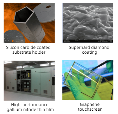
Figure 3: Applications of CVD technology
7.Applications of Chemical Vapor Deposition (CVD) in Noble Metal Materials
1. Production of Noble Metal Thin Films:
Noble metal thin films have attracted researchers' interest due to their excellent oxidation resistance, high electrical conductivity, strong catalytic activity, and exceptional stability. Compared to other methods for producing noble metal thin films, chemical vapor deposition offers more technical advantages, making it the preferred approach for most applications. The deposition precursors used for noble metal thin films are diverse, but mainly include halides and organic compounds of noble metal elements, such as carbonyl chloride, chlorocarbonyl platinum, chlorocarbonyl iridium, and cyclopentadienyl complexes, among others.
In a specific research, a team explored the feasibility of using noble metal thin films as electrode materials on substrates like sapphire, quartz glass, and yttria-stabilized zirconia (YSZ). During the chemical deposition process, oxygen was introduced into the system to eliminate carbon generated from the thermal decomposition of the precursors. This resulted in noble metal thin films with a metallic luster. Otherwise, carbon-encapsulated iridium nanoparticles, referred to as iridium-carbide clusters, would be obtained. The deposited iridium-carbide clusters on YSZ exhibited excellent electrical performance and catalytic activity. At relatively low temperatures, the interface conductivity of the iridium-carbide clusters reached more than a hundred times that of pure iridium or platinum. The use of noble metal-carbon clusters as highly porous catalytic membranes in electrode materials holds promising potential for future applications.
2. Production of Noble Metal Iridium High-Temperature Coatings:
In the 1980s, NASA began using metal-organic compounds through chemical vapor deposition to successfully produce composite nozzles coated with rhenium-based iridium. This marked a breakthrough in the application of chemical vapor deposition in the production of noble metal coatings.
NASA utilized acetylacetonate (C15H21IrO6) as the precursor for the iridium coating, and the deposition was achieved through the thermal decomposition reaction of acetylacetonate. The deposition rate of iridium was fast, reaching up to 3~20 μm/h, and the deposition thickness reached 50 μm. The efficiency of acetylacetonate synthesis was over 70%.
3. Palladium (Pd) Chemical Vapor Deposition:
Pd and its alloys have strong adsorption and selective permeability for hydrogen, making them ideal materials for hydrogen storage or purification. Pd is mainly used in the production of hydrogen purification equipment as Pd alloys or Pd coatings. Some researchers have also used chemical vapor deposition to produce Pd thin films or coatings. This is achieved by using metal-organic compounds with extremely low decomposition temperatures as Pd precursors. Examples include allyl [β-ketoimine] Pd(II), Pd(η-C3H5)(η-C5H5), and Pd(η-C3H5)(CF3COCHCOCF3). This method can produce Pd thin films with high purity.
With the continuous improvement in the requirements of aerospace, nuclear industry, semiconductors, and other fields for semiconductor devices, integrated circuits, high-field and small-sized superconducting materials, and crystal growth products, chemical vapor deposition technology has a broad market application prospect as an essential method for material preparation and effective surface modification. Some researchers predict that CVD will focus on reducing harmful by-products and increasing industrial-scale production in the future. Additionally, the development of lower-temperature CVD processes, more precise control over CVD processes, thick film deposition techniques, novel film materials, and new material synthesis technologies will be the major areas of research in the future.
Scan the QR code to read on your phone
Hot Technology Ranking

2022-10-20

Scan the QR code and follow the official account
Products
Precious metal functional materials
High-quality optoelectronic materials/high-purity targets
Refractory metals and their alloys
Special alloy/special steel
Spherical | Nano powder
Biomedical/3D printing products
Compound
Rare metals and their alloys
Rare metals and their alloysRare Metal Concept Cultural/Art/Collectible
Nuclear energy Nuclear power Nuclear industry
High temperature heat container
Microelectronics industry Chip thermal sink
Semiconductor equipment MOCVD thermal field
High efficiency & long life Wire for wire cutting
Medical equipment Medical instruments
Artificial bone joint Bioimplantation
Rare metal cultural & creative art collection Precious metal
Plasma|Special Welding Electrode
Ultra Minor Metals Ltd (UMM) all rights reserved 湘ICP备17001881号 by:www.300.cnchangsha