Industry News
Learn more about us through the industry
News
Ru sputtering target factory Introduction Product categories
- Categories:News
- Author:
- Origin:
- Time of issue:2023-03-16 10:51
- Views:0
(Summary description)Ru sputtering target factory tells you the types and classifications of sputtering targets.
(1) According to the chemical composition and material of the target, the sputtering target can be divided into metal/non-metal single substance target, alloy target, ceramic/compound target, etc.
Ru sputtering target factory Introduction Product categories
(Summary description)Ru sputtering target factory tells you the types and classifications of sputtering targets.
(1) According to the chemical composition and material of the target, the sputtering target can be divided into metal/non-metal single substance target, alloy target, ceramic/compound target, etc.
- Categories:News
- Author:
- Origin:
- Time of issue:2023-03-16 10:51
- Views:0
Ru sputtering target factory tells you the types and classifications of sputtering targets.
(1) According to the chemical composition and material of the target, the sputtering target can be divided into metal/non-metal single substance target, alloy target, ceramic/compound target, etc.
(2) According to different target shapes, there are mainly long targets, square targets, round targets and tube targets.
(3) According to the classification of application fields, there are mainly targets for semiconductors, targets for flat panel displays, targets for solar cells, etc.

Main application fields and technical requirements of sputtering targets.
chip field.
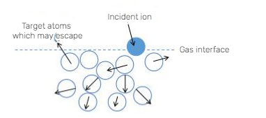
The purpose of selecting metal sputtering targets for semiconductor chips is to make metal wires for transmitting information on the chips. First, the high-speed ion flow is used to bombard the surface of different types of metal sputtering targets under high vacuum conditions, so that atoms on the surface of various targets are deposited on the surface of the semiconductor chip layer by layer, and then passed through the The special processing technology etches the metal film deposited on the surface of the chip into nanometer-scale metal wires, and connects the hundreds of millions of micro transistors inside the chip to transmit signals.
Ru sputtering target factory will introduce to you: With the rapid development of information technology, the requirements for integrated circuits are getting higher and higher, and the size of unit devices in the circuit is continuously shrinking, and the size of components is from millimeters to microns, and then to nanometers. Each unit device is composed of substrate, insulating layer, dielectric layer, conductor layer and protective layer.
Scan the QR code to read on your phone
Top dynamic rankings


Scan the QR code and follow the official account
Products
Precious metal functional materials
High-quality optoelectronic materials/high-purity targets
Refractory metals and their alloys
Special alloy/special steel
Spherical | Nano powder
Biomedical/3D printing products
Compound
Rare metals and their alloys
Rare metals and their alloysRare Metal Concept Cultural/Art/Collectible
Nuclear energy Nuclear power Nuclear industry
High temperature heat container
Microelectronics industry Chip thermal sink
Semiconductor equipment MOCVD thermal field
High efficiency & long life Wire for wire cutting
Medical equipment Medical instruments
Artificial bone joint Bioimplantation
Rare metal cultural & creative art collection Precious metal
Plasma|Special Welding Electrode
Ultra Minor Metals Ltd (UMM) all rights reserved 湘ICP备17001881号 by:www.300.cnchangsha


